|
Part No:MPCHH-FPGA-DIGI-LOGIC
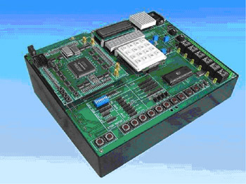
System Features of the
CPU BOARD (download board):
1. It supports
ALTERA-EP1C6(240PIN) VLSI
2. System chip
produced with 0.13 semiconductor process, maximum speed is 240MHz
3. 3.3V
voltage is used, 2.5V core voltage: Multi Voltage 3.3 / 2.5 / 1.8 / Vref
4. All inputs
and outputs should have high voltage conversion bus.
5. The
software platform should be QuartusII: Suitable for the latest software
platform Quartus II of ALTERA
˙
It Supports 5,980 logic cells (approx. 120,000
logic gate counts)
˙The
Maximum capacity of Memory bit can be up
to 92,160 bit; uses M4K
(similar to Stratix’s
structure) for memory structure.
˙
It
Supports the design of 2 PLL (Pulse-phase Lock Loop), can be used for
frequency increase and phase adjustment of the pulse.
˙
It Supports 8 sets of global clock for user definition; it adopts the
hierarchy
configuration of clock tree.
˙
It Supports low-cost serial configuration
device to achieve FPGA device
programming.
˙ It
Supports LVTTL, LVCMOS, SSTL-2 and SSTL-3 I/O interface standard.
˙ It
Supports 66-MHz, PCI of 32-bit interface standard.
˙ It
Supports low-speed, low-voltage differential signal, LVDS (311 Mbps) I/O
interface standard.
˙It
Supports external memory of 133MHz DDR SDRAM, FCRAM and SDR
SDRAM memory I/O interface standard.
˙CPU
system board can be performed independently, and built in Download
Cable (Circuitry) is provided for project
development.
˙The
main board provides 2 independent power sources of 5V/3.3V, support
the
chips from different manufacturers
˙The
protection against short circuits and overloading is equipped.
˙It
has a special programmer for the CPLD/FPFA, no additional programmer is
needed.
˙176
I/O pins in total are expandable, it’s very convenient to be connected to
breadboard for the purpose of the integrated applications of CPLD/FPGA
combined with 8051,AVR,PIC.
˙The
main board contains 4 sets of oscillating frequencies: one is fixed
frequency, the others are adjustable. The user can switch them from
one to
another.
˙User
can use GRAPHIC/VHDL/Verilog or related
graphic or Hardware
Description
Language to
implement circuit design.
The I/O Interface experiment
The parts of Input
/ Display / Comprehensive Application
1. Experiment of LCD Call
Display.
2. Experiment of incoming
calling.
3. Experiment of VGA
ping-pong ball game software module
4. Experiment of PS2
interface
5. Experiment of Mouse
interface
6. Experiment of Keyboard
interface
7. Experiment of
Photo-coupler I/O module
8. Experiment of 8051 module
9. Experiment of RAM memory
module
10. Experiment of ROM memory
module
11 Experiment of Push-button
on/off module.
12. Experiment of Download
module
The parts of
Special Applications
˙24
bits VGA port x 1
˙PS/2
port x 2
˙Digital
audio plug x 1.
˙Includes
three 8 bit D/A converter to support
80 MSPS Operation.
˙Diversity
YPbPr/GBR input modes of can be Three 8 Bit 4:4:4, Two 8 Bit
4:2:2 or One 8
Bit 4:2:2
˙Supports
Bi-Level (EIA) or Tri-Level synchronous signals of
Society of Motion
Picture and Television Engineers (SMPTE)
˙The
ratio of Video / synchrony is 7:3
˙SYNC
signal can be used to accumulate to green/brightness analog video
output or
all analog output signal.
˙Configurable
blanking signal.
˙Internal
reference-level (voltage) is available.
˙PS2
interface.
˙Audio
output plug
˙High
definition television (HDTV) video converter box/receiver.
˙High
resolution image management
The Special Features of Interface card
This interface card V01 can
support multi-digital video input including diversity YPbPr/GBR digital
video formats of Three 8 Bit 4:4:4, Two 8 Bit 4:2:2 or One 8 Bit 4:2:2 of
(ITU-BT.656). The output can generate R/G/B 24 bit high resolution colour
signal output via VGA port.
The interface card V01 also
equips with audio output, this will be able to broadcast user-defined
digital buzz signal
The
interface card V01 contains a chip that with built in three sets of high
speed 8 bit D/A Converter (DAC)
developed by Texas Instruments (TI). This component can be operated under
the environment of 5V analog voltage and 3V to 5V digital voltage, the
maximum sampling rate is 80MSPS. By using digital controlled interface, the
conventional bi-level synchronous signal or
tri-level synchronous signal that conform to
Society of
Motion Picture and Television Engineers (SMPTE)
can be generated. Such synchronous signal can be accumulated to the singular
analog output signal channel (AGY) (syc-on-green / luminance) or to all the
analog (AGY/ARPr/ ABPb) output channel. The ratio of video to synchronous
potential is 7:3. The interface card V01 also integrates PS2 and its audio
output plug to control the mouse and keyboard or outputting video and audio
signals simultaneously. It’s very suitable for teaching, as well as for
practical applications. |